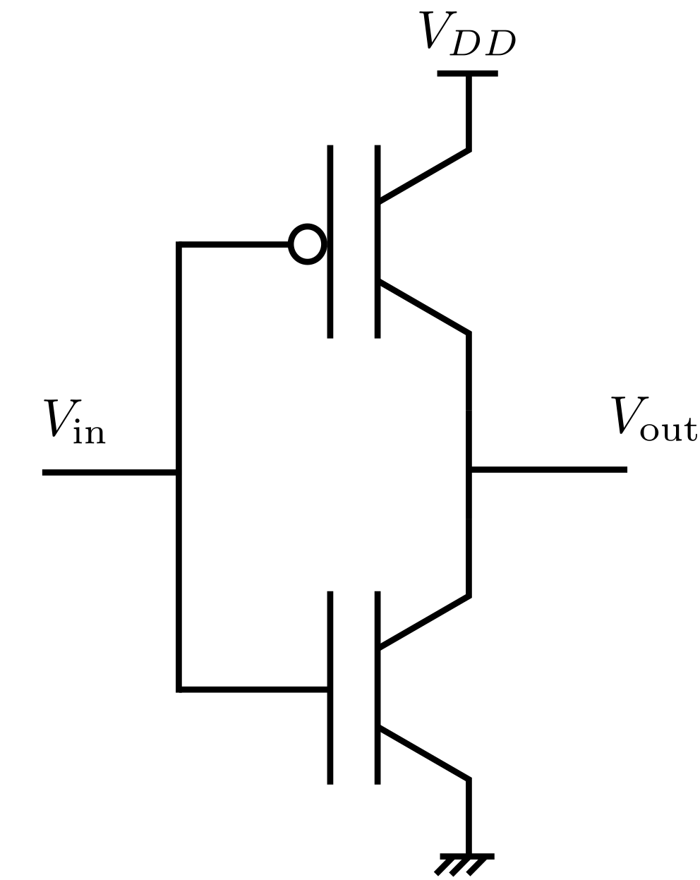
I am confused by a litte detail with CMOS inverter. Note that I am really a beginner in CMOS "theory". Here is the electrical circuit:
At "first view", I understand the principle. If \$V_{in}\$ is high (\$V_{in}=V_{DD}\$), then the PMOS will be open and the NMOS closed. Thus \$V_{out}=0\$.
Reciprocally, \$V_{in}=0\$ implies the PMOS closed and NMOS closed thus \$V_{out}=V_{DD}\$
My question
I have trouble when I look at the details. Let us consider \$V_{in}\$ high for instance. A PMOS will be closed for \$V_{GS} < V_{Tp}<0\$ (threshold voltage), and \$V_{GS} > V_{Tn}>0\$ for NMOS.
But for this I must identify where are source and drain. To identify where is the source and the drain of a transistor, I must find which one has the highest voltage.
But as I do not know \$V_{out}\$ how can I find them ? \$V_{out}\$ is what I try to find so I am not supposed to know it (else the reasoning is circular)...
Is there an implicit assumption that "by design", for CMOS circuit, any voltage in the circuit will verify \$0 < V < V_{DD}\$. Applying this to \$V_{out}\$ I can deduce source and drain for both transistors and solve my issue ?
Because "in principle", I could imagine some negative voltages and because of that identifying what is source and drain is not straightforward here.


\$<stuff>\$to make latex work properly. You drew the schematic so you label where source and drain need to be. There is a right way and a wrong way BTW. \$\endgroup\$But for this I must identify where are source and drain. To identify where is the source and the drain of a transistor, I must find which one has the highest voltage.No, to identify source and drain you must know whether you have a P or N channel device, and then source is the common terminal of the inverter that that device forms, so the two sources connected to GND and VDD, the two drains go to the output. \$\endgroup\$