3
\$\begingroup\$

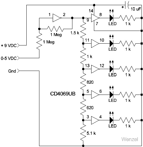
I saw this schematic and I had problems finding out how it works:

CD4069 LED bar graph

As the voltage increases from zero, the first LED grows in brightness. Just when that LED is fully lit, the next LED begins to glow slightly. Each LED represents about 1 volt of change, when the circuit is operating from 9 volts.

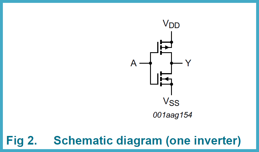
According to the 4069 datasheet, the gates are not Schmidt triggers nor buffered, and the diagram for a gate seems quite simple:

a single 4069 gate

If I'm right, the resistors form a voltage divider and just drive the LEDs.

I have these questions:

  1. How does the circuit work? Why doesn't the next LED light up until the previous one is fully lit?
  2. What does the first gate (left most gate, with two 1Mohm resistors) do?
  3. What kind of modifications do I have to do, to make it work with a 5V supply? The supply would be a constant 5V and the input would be a variable 5V.

regards.

\$\endgroup\$

2 Answers 2

5
\$\begingroup\$

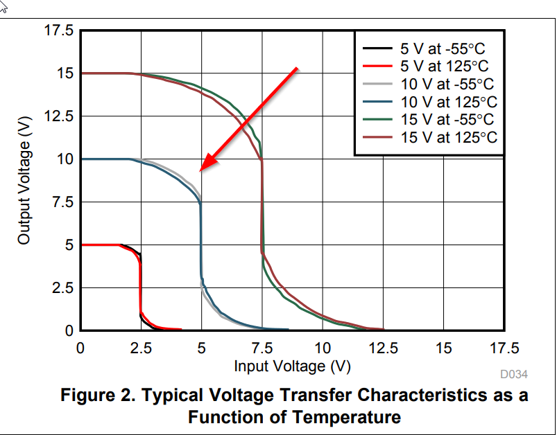
Have a look at the typical characteristics of a CD4069UB gate:

enter image description here

As you can see, the gate with no feedback (typically) acts as crude comparator that switches at approximately Vdd/2 (which is 4.5V in this case).

With feedback it can be considered an amplifier with a transfer function as follows:

Vpin1 = 4.5V, Vpin1 = (Vo + Vin)/2 => Vo = 9V-Vin

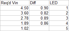
Now we can easily calculate the transition voltage for each LED from top to bottom, since it's a simple voltage divider (the gate inputs draw negligible current):

enter image description here

The right-hand column indicates the difference to the next LED, which is fairly constant.

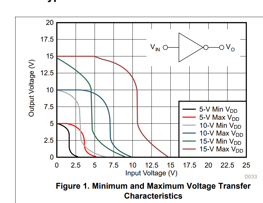
It should be mentioned that this circuit works "typically" and there is no guarantee that any given gate will behave that way, in fact if you look at the worst-case characteristics:

enter image description here

.. it may not work very well at all. Also both the transistors are partly 'on' at the transitions (and the input gate is biased so it also has both transistors on) so the circuit draws extra mA that are wasted.

So it's an okay toy, but not really something you'd want to ship.


To make it work from a 5V supply, you can simply reduce the supply voltage and accept that the input voltage will be scaled proportionally. Instead of 0..5V it will be more like 0..2.8V. Use a divider at the input if you want a 0..5V approximately input voltage. There is no control over how 'sharp' the transitions are, you're at the mercy of the physics and fabrication of the inverters.

\$\endgroup\$
7
\$\begingroup\$

This circuit relies on the fact that the CD4069, as well as all other "digital" logic ICs, are not really digital but analog electronics operating (usually) at the extremes of saturation and cutoff. But they can be operated linearly. Usually this is undesired operation but for an example like this, it can be useful.

The 5 individual inverters are operated as amplifiers in their linear mode until they reach either saturation on the way up or cutoff on the way down. The resistor in the "ladder" are carefully sized so that the saturation of one corresponds with the start of the linear region of the one above it.

It's easy to just assume that all circuits always behave linearly but they don't. That's a simplification to make designing digital circuits simpler.

\$\endgroup\$
2
  • \$\begingroup\$ What does the first gate do ? \$\endgroup\$ Commented Feb 20, 2021 at 18:33
  • \$\begingroup\$ It's acting as an inverting amplifier, Note the feedback resistor just as you'd have with an opamp circuit. In this case there is no non-inverting input but it doesn't matter as that would normally be tied to ground. \$\endgroup\$
    – jwh20
    Commented Feb 20, 2021 at 18:34

Your Answer

By clicking “Post Your Answer”, you agree to our terms of service and acknowledge you have read our privacy policy.

Not the answer you're looking for? Browse other questions tagged or ask your own question.