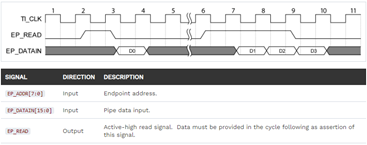
I am trying to run Vivado's implementation on my design but I am getting this error: [DRC MDRV-1] Multiple Driver Nets: Net pipea0/ep_read has multiple drivers: pipea0/ep_read_INST_0/O, and rd_en_reg/Q. When I was running synthesis, I got an error saying that I could not connect .ep_read to the register rd_en. I think this error was coming from rd_en being a register when it should have been a wire so it could be instantiated in the okPipeOut module. In order to fix this I tried to create another wire called rd_en_connect and then I assigned my rd_en register to that wire.
I now think that the implementation error I am getting is the same error I was getting during synthesis. I am not sure how to fix this error since I need rd_en to be a register. Is there a simple way to fix this error? If not, how can I keep the same functionality but define rd_en as a wire?
In brief, I am using a counter to measure the pulse width of an incoming signal (in_1) and then multiply the counter output by the clock period to get the pulse width with respect to time. I am then using Vivado's FIFO generator with separate write and read clocks to cross the clock boundary between the FPGA and my PC so I can see the pulse measurements in an output file. Modules okHost, okWireOut and okPipeOut are all preloaded modules that come with my FPGA.
`timescale 1ns / 1ps

module Pulse_counter(
input in_1  ,                     // input signal
output reg [15:0] count_out,      // output of the counter

input [4:0] okUH,      // Input from Opal Kelly USB controller (from PC)
output [2:0] okHU,     // Outputs to Opal Kelly USB Controller (to PC)
inout [31:0] okUHU,    // Bidirectionals to USB Controller
inout okAA
);

    wire okClk;            // Clock used synchronize FPGA to the Opal Kelly modules (?)
    wire [112:0] okHE;     // Opal Kelly module address and control bus
    wire [64:0] okEH;      // Outputs from the various OK modules back to the okHost core
    wire reset;
    reg [15:0] counter;
    reg rd_en;
    wire rd_en_connect;
    reg wr_en;
    wire empty;
    wire full;
    wire [15:0] dout;
    wire wr_ack;

    reg in_1_del;
    wire in_1_ne = !in_1 & in_1_del; // Negative edge of in_1
    reg in_del_ticlk;
    wire rd_trig = !in_del_ticlk & ti_clk; // Write enable trigger

assign rd_en_connect = rd_en;

initial counter = 16'b0;
initial wr_en = 1'b0;
initial rd_en = 1'b0;

fifo_generator_0 myfifo (
  .wr_clk(okClk),      // input wire wr_clk connnected to the Opal Kelly FPGA clock
  .rd_clk(ti_clk),     // input wire rd_clk connected to the USB's clock
  .din(count_out),     // input wire [15 : 0] din connected to the pulse measurement
  .wr_en(wr_en),    // input wire wr_en
  .rd_en(rd_en),    // input wire rd_en
  .dout(dout),      // output wire [15 : 0] dout
  .full(full),      // output wire full
  .empty(empty),    // output wire empty
  .wr_ack(wr_ack),  // output wire wr_ack confirms that a write request succeeded during the last write clock
  .valid()          // output wire valid indicates valid data is available on output bus (dout)
);


okHost okHI(
    .okUH(okUH),
    .okHU(okHU),
    .okUHU(okUHU),
    .okAA(okAA),
    .okClk(okClk),
    .okHE(okHE),
    .okEH(okEH)
);

okWireIn endpoint00(
    .ep_addr(8'h00),
    .okHE(okHE),
    .ep_dataout(reset)
);

okPipeOut pipea0(
     .okHE(okHE),
     .okEH(okEH),
     .ep_addr(8'ha0),
     .ep_read(rd_en_connect),
     .ep_datain(dout)
);

always @(posedge okClk) begin
    if (reset || counter==16'hFFFF) begin
        counter <= 16'b0 ;         // If reset is high reset the counter to 0
    end
    else if (in_1) begin
        counter <= counter + 1;    // As long as input is high keep counting
    end
    else if (in_1 == 16'b0) begin
        if (counter !== 16'b0) begin    // Without this block the output was set to the counter
            count_out <= 5*counter;     // value for only one clock cycle before it was reset back to zero
        end
        counter <= 16'b0;           // Reset counter once the input signal returns back to zero
    end
end

always @(posedge okClk) begin
    if (reset) begin
        in_1_del <= 1'b0;
    end else begin
        in_1_del <= in_1;        // Delayed input signal by one okClk cycle
    end
end

always @(posedge okClk) begin
    if (reset || full) begin
        wr_en <= 1'b0;
    end else begin
        wr_en <= in_1_ne;        // Assign the write enable to the negative edge of in_1
    end
end

always @(posedge ti_clk) begin
    if (reset) begin
        in_del_ticlk <= 1'b0;
    end
    else begin
        in_del_ticlk <= in_1_del;    // Delay the delayed input signal by one ti_lk cycle
    end
end

always @(posedge ti_clk) begin
    if (reset || empty) begin
        rd_en <= 1'b0;
    end else begin
        rd_en <= rd_trig;        // Assign read enable to its trigger
    end
end


endmodule
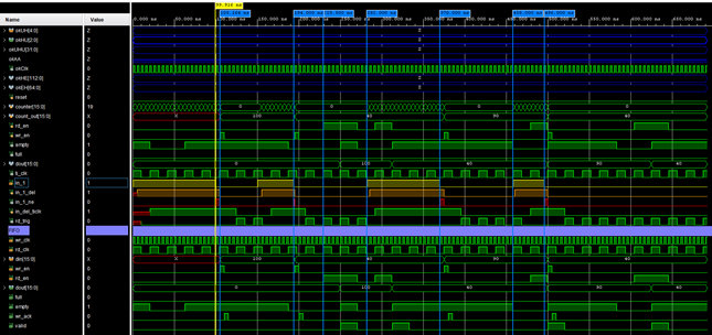
Here is a simulation result I got before I had to add the rd_en_connnect wire.


