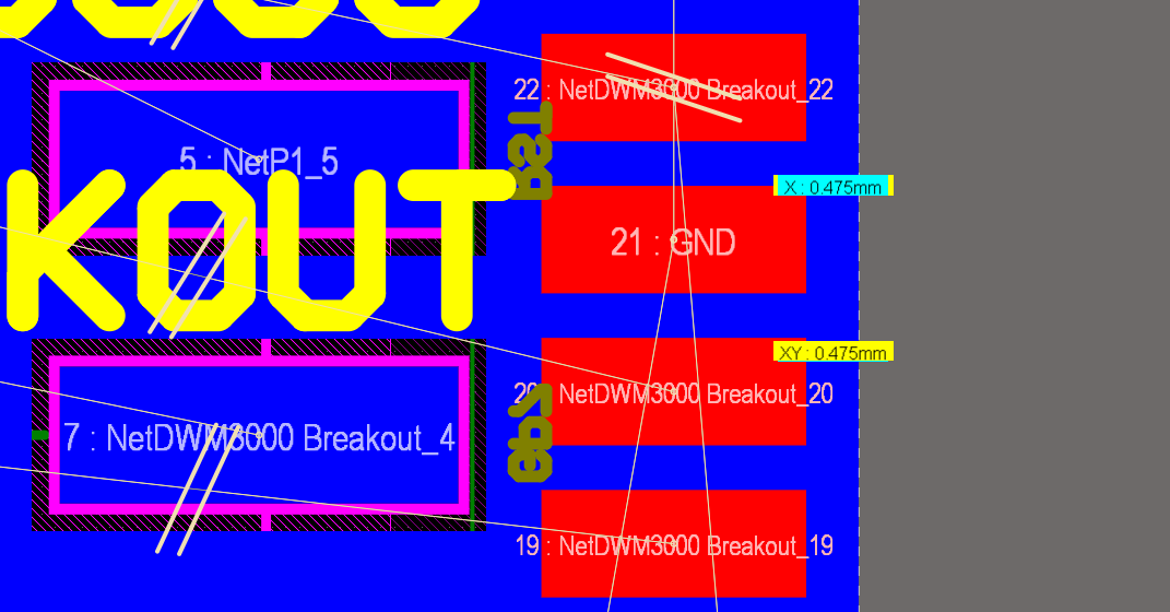
Working with very limited space (In Altium) and need to place vias to make routes between the red solder castellation plates on the top layer to the respective connector pins on the bottom layer, both shown in the image. Since I have only 0.475mm clearance between the edge of the plates and the edge of the board and need to place the vias in front of the red plates, how small can I effectively make the diameters of my vias? Why does the size even matter?
-
5\$\begingroup\$ This question has got nothing to do with Altium and everything to do with how much you want to pay for the finished PCB and who the manufacturer of the PCB is. \$\endgroup\$– Andy akaCommented Mar 2 at 11:40
-
1\$\begingroup\$ @Andyaka I only mention Altium as that's the system I'm using and for which I'm seeking advice. What I'm trying to ask is, does the diameter matter for anything other than cost. I would assume that the smaller I make it and the tighter the clearances are, the more expensive it would be. \$\endgroup\$– eutectic_codswallopCommented Mar 2 at 11:48
-
\$\begingroup\$ I'm not going to make this an answer as others have covered the detail adequately. But I do want to emphasize the importance of, in a case like this, choosing your PWB manufacturer first, based on your needs and their capabilities. Note also that even within a given vendor, different locations/factories may have different capabilities. \$\endgroup\$– SteveShCommented Mar 2 at 12:09
-
\$\begingroup\$ Low cost prototyping services tend to have a minimum around 450um for the ring and 200um for the drill, but it really depends who is making it and how much you're willing to pay. \$\endgroup\$– user1850479Commented Mar 2 at 13:10
-
\$\begingroup\$ Will you be hand soldering or producing a small quantity of boards? If so, just put the via in the pad! \$\endgroup\$– AttieCommented Mar 2 at 14:12
4 Answers
Look at the 'capabilities' of your PCB manufacturing house. Mechanical drills are used for relatively large holes. Very small drills will result in a higher cost. For extreme tiny holes (like 100um) laser drilling is used, which is more expensive.
Once you have the hole size, there needs to be a minimum annular ring around the hole. Again there may be more than one possible choice of minimum with a higher price associated with a smaller ring. Sometimes the manufacturer will have a specific via minimum specified that is a bit tighter than for through-hole pads.
You may be concerned about the current capability or electrical resistance of the via, which may point to a larger size.
Creating a vast sea of functional (say not just stitching vias which will test as good even if a few are not) vias at the absolute minimum via size may affect manufacturability and the manufacturer may ask for more money or refuse the job (as they sometimes do when someone creates a coil at the minimum trace/spacing dimensions) because yield will suffer.
It should also be noted that usually extreme small via sizes, thin traces etc. are associated with boards with many layers (eg. HDI boards) and are generally made in a separate facility from cheap 2/4 layer boards. As such you can easily see one or two orders of magnitude price difference for a similar size board- sometimes three, depending on the quantity and what kind of pricing structure they have. So a $20 order may turn into a $1500 order because you're paying for all that capability in that facility.
Of course you can draw whatever size via you want in an EDA program like Altium (down to some extreme tiny resolution in PCB context, and Gerber files have some resolution due to the number of digits used) however there are 'Design Rules' that you generally set before beginning that will be used to check that what you are creating meets the capabilities of your selected gamut of fab houses.
-
\$\begingroup\$ As another data point I happened to find myself in a high-end Berlin prototype facility a few days after posting this, and they mentioned they could make mechanically drilled vias as small as 50 microns. \$\endgroup\$ Commented Apr 5 at 22:33
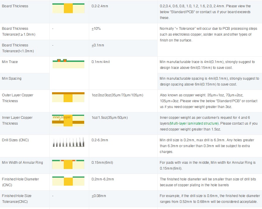
When initiating a design, it's crucial to assess the capabilities of the factory responsible for manufacturing your PCB. The minimum size of vias is typically provided in the manufacturer's capability section on their website. It's important to note that smaller via-hole sizes can increase the production cost of your board. For instance, if you're considering PCBWAY Company for production, you should review the information provided in the link I've included.
Picture reference: https://www.pcbway.com/capabilities.html
And it's important to note that the size of the via holes is determined by the PCB manufacturing company, and designers cannot freely choose any size they want in their designs.
Picture reference: https://www.pcbway.com/capabilities.html
Nevertheless, you can contemplate utilizing via hole diameters of up to 0.2 and a ring size of 0.45, tailored to suit your specific application requirements.
Working with very limited space (In Altium) and need to place vias to make routes between the red solder castellation plates on the top layer to the respective connector pins on the bottom layer, both shown in the image. ..., how small can I effectively make the diameters of my vias?
Other answers have given good information answering the question as asked, but this might be an X-Y problem. You have to get the signal from the top to the bottom in limited space, so you've decided the solution is to make the vias as small as possible.
I'm assuming you can't just move the component away from the board edge to give you more space, because that's a pretty obvious solution also.
But have you considered just using via-in-pad technology? To do this, you would drill an ordinary-sized (8 mil / 0.2 mm or larger) via through the middle of the component pad. Then the via is filled with epoxy and copper is plated over it so that the pad doesn't have a void in it. This does add some cost, but it is probably not as much as trying to drill holes below 8 mils.
Any shop capable of drilling 8 mil (or lower) vias these days should also be capable of doing via-in-pad.
How To
The usual way to produce via-in-pad is to place the vias in Altium with a unique size, for example 8.1 mils instead of 8 mils. Then a fabrication note something like "vias indicated as 8.1 mils are via-in-pad plated over". If you are designing for high volume production you can add a spec for the flatness of the resulting pad and for the type of the epoxy fill.
-
\$\begingroup\$ So placing a via in a pad is simple as just dragging the via over the top of the pad? \$\endgroup\$ Commented Mar 3 at 8:46
-
\$\begingroup\$ @eutectic_codswallop, as far as Altium is concerned, yes. But you should also make sure to communicate with the fab shop (through the notes/drawings) that via-in-pad process is required. \$\endgroup\$ Commented Mar 3 at 15:49
In your case, with only 0.475mm clearance between the edge of the plates and the board edge, you should consider the following:
Ensure that the vias are placed with enough clearance to avoid any unintended electrical connections or signal distortions. Consult with your PCB manufacturer to determine the smallest viable via size based on their capabilities. Consider using blind or buried vias if available to save space and improve routing efficiency.


