0
\$\begingroup\$

The problem is an inconsistency I observed when I compared the result of the synthesis step to the result of the P&R step. The P&R inserts a combinatorial loop which is not present in the synthesis step. The tool flags then for the loop issue in the P&R trace report. I could make the problem disappear by resetting the variable properly but I haven't really grasped why the loop buffer is inserted.

I simplified the VHDL code in question for the purpose of this post. It is a legacy code that resets an internal variable to the value of an input pin, which I suspect to be a bug.

ENTITY InjectCtrl IS
  PORT
  (
    Reset    : in STD_LOGIC;
    clk      : in STD_LOGIC;
    inject   : in STD_LOGIC;
    injector_opens  : out STD_ULOGIC;
    injector_closes : out STD_ULOGIC
  );
END ENTITY;

architecture rtl of InjectCtrl is

begin

  Process(Reset, clk)
    Variable Delayed_Inject : STD_LOGIC;
  Begin
    if reset = '0' then
        injector_opens <= '0';
        injector_closes <= '0';
        Delayed_Inject := '0';
        Delayed_Inject := Inject; -- issue line
    elsif rising_edge(clk) then
        injector_opens <= '0';
        injector_closes <= '0';

        if (Delayed_Inject = '0') then
            injector_opens <= '0';
            injector_closes <= '1';
        else
            injector_opens <= '1';
            injector_closes <= '0';
        end if;

        Delayed_Inject := Inject;
    end if;

  end Process;

end architecture;

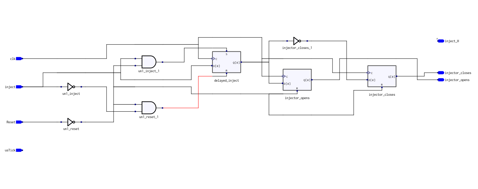
The generated RTL diagram looks like this.

RTL view

The diagram seems to be in line with what the code is specifying. The variable Delayed_Inject samples the value of the inject input every clock cycle, hence the flip-flop. However when the reset signal is de-asserted (reset = '0'), the variable is not set to '0', but instead to the value of the input signal inject. This explains why inject is routed through logic to the SET pin of the flip-flop. So at reset, if inject input is high, RESET pin is low and SET pin is high, which results in an output from the flip-flop being also high. Inversely, if inject is low, RESET pin is high and SET pin is low which gives a low output (D FF with set and reset pin).

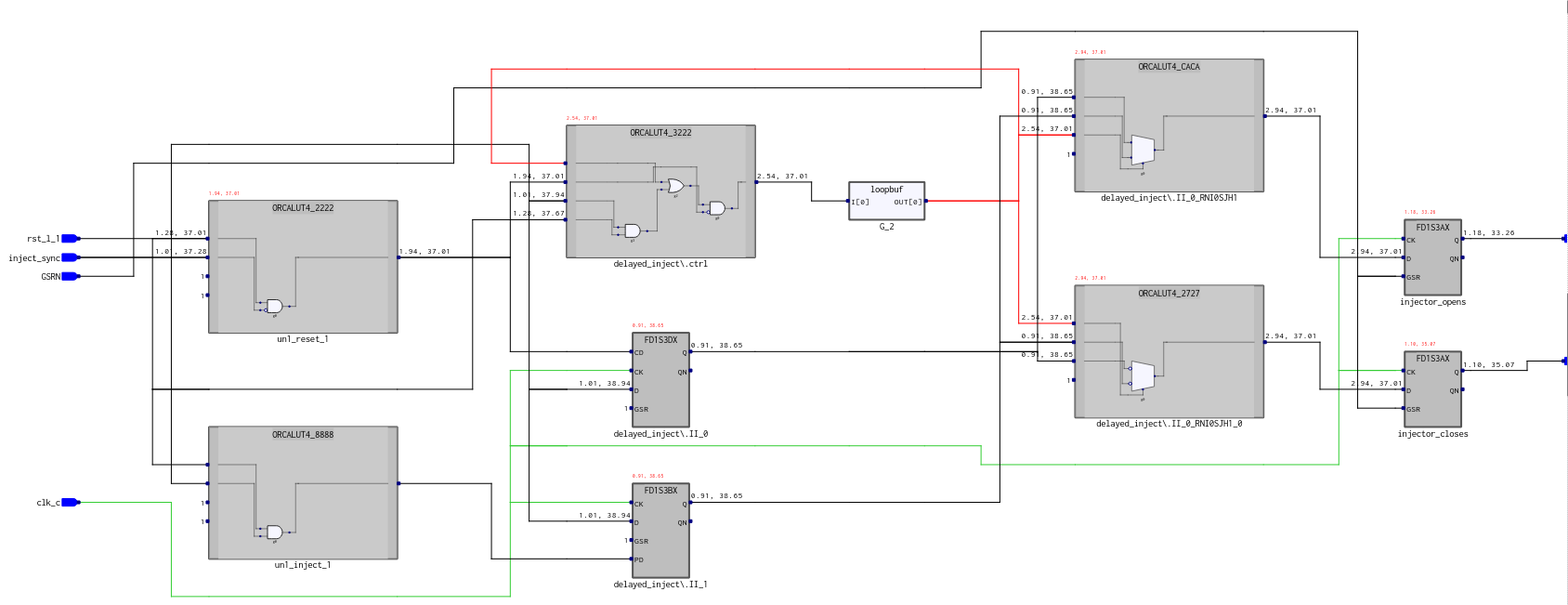
The technology view diagrams looks a bit different from what I have expected.

enter image description here

First, notice the inference of two flip-flops for Delayed_Inject instead of one. But what is most interesting is the inference of a loop buffer that is routing the output of the LUT_3222 to itself. Where does that loop come from?

For reference, I am using Lattice Diamond with Synplify as synthesis tool of choice. The target FPGA is from the LFE5U family.

\$\endgroup\$
2
  • \$\begingroup\$ Two things: 1) try not to use variables. They are virtual values and depending on the context, the synthesizer will try to make something of it, but the result can be inconsistent. Just use a signal. 2) try to use synchronous reset logic. It also prevents all kinds of running challenges for the synthesizer. \$\endgroup\$
    – JHBonarius
    Commented Aug 5, 2022 at 10:30
  • \$\begingroup\$ In the state of the art way of FPGA VHDL designing, the reset value of a signal is assigned to a given value, a constant or a constant coming from a generic parameter. But not from a port like you did. So the tool must infer comb to implement what you coded \$\endgroup\$
    – user282292
    Commented Aug 5, 2022 at 19:09

1 Answer 1

1
\$\begingroup\$

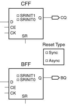
I believe the discrepancy you are seeing is down to the RTL diagram being technology-independent. It correctly interprets your code, and shows a register with an async 'load' function, implemented by asserting either the set or reset pin of the flip-flop (again, as per your code). Your physical device likely doesn't have this capability. I could not find an equivalent diagram for Lattice ECP5, but a Xilinx one looks like this:

Xilinx Spartan 6 CLB FF reset capabilities1

The register has one SR input, that can, at compile time, be configured to either set the register to '0' or '1', and to be either 'sync' or 'async'. As you can see, this does not directly facilitate an async load function such as the one in your code. As a result, the mapper tool has to find 'some other way' to implement what you have asked for, and a combinatorial loop has resulted.

The best solution in my opinion is to convert the code to implement synchronous reset functionality, as suggested in a comment. If this isn't possible, perhaps the external reset input can be resyncronised.

\$\endgroup\$
2
  • \$\begingroup\$ As I mentioned in my comment (before migration), the external reset is indeed synchronized with the clock, whilst modules are implemented with async reset. I am not very familiar with Xilinx but looking at their primitive library, it should be possible to implement the desired async load function by using one FDPE (async preset) and one FDCE (async clear), then selecting one from two outputs depending on the value of inject. This can be done without inferring a loop. It is really the loop inference that I can't understand. \$\endgroup\$
    – Theo
    Commented Aug 8, 2022 at 10:57
  • \$\begingroup\$ @Theo I suppose you could manually instantiate those primitves to create the circuit you want and if the tools are happy and it works OK, that could be your solution. My only thought is whether this could result in a race condition or glitches on the output; perhaps these wouldn't matter in your case. \$\endgroup\$
    – scary_jeff
    Commented Aug 15, 2022 at 8:00

Your Answer

By clicking “Post Your Answer”, you agree to our terms of service and acknowledge you have read our privacy policy.

Not the answer you're looking for? Browse other questions tagged or ask your own question.