1
\$\begingroup\$

I'm trying to implement a shift register and therefore need values to be stored on the downwards edge of the clock signal (otherwise the whole register just sets to the input), so I am using a master-slave D-type flip-flop to store each bit. The design also requires a control line that resets the value stored in each flip-flop to 0 (low voltage) regardless of the clock value. How would I implement this by editing the below circuit?

schematic

simulate this circuit – Schematic created using CircuitLab

\$\endgroup\$
9
  • \$\begingroup\$ Any reason why you haven't used a DFF logic IC but have made it out of NAND gates instead? It would be straightforward to implement reset otherwise and you'd be making a simpler circuit. \$\endgroup\$
    – TonyM
    Commented Nov 21, 2016 at 12:46
  • \$\begingroup\$ @TonyM I'm not an electrical engineer, I'm a computer scientist! I need to use just logic gates for my circuit. \$\endgroup\$
    – Rob Murray
    Commented Nov 21, 2016 at 15:12
  • 1
    \$\begingroup\$ There's no difference between using a logic IC or using individual gates to get from point A to point B except that if you use a chip you'll have a lot less wiring - and the joys that go with it - to contend with. :) \$\endgroup\$
    – EM Fields
    Commented Nov 21, 2016 at 15:19
  • 1
    \$\begingroup\$ But you will have to make your circuit out of many more logic ICs than if you used a D-type flip-flop logic IC. Sorry, it seemed a fair question. \$\endgroup\$
    – TonyM
    Commented Nov 21, 2016 at 15:19
  • 1
    \$\begingroup\$ Good for you, to be encouraged :-) I did electronics at college and computer science at uni, found that they complemented each other well. Electronics design became the forte. Anyway, let me think about this question. \$\endgroup\$
    – TonyM
    Commented Nov 21, 2016 at 21:05

2 Answers 2

3
\$\begingroup\$

An asynchronous reset can be implemented by adding a third input to the lower NAND gate in each of the cross-coupled pairs in your diagram. Connect them together and drive this input low to reset the output; otherwise, drive it high.

BTW, it would have been easier to talk about the individual components of your diagram if you had left the reference designators on them.

\$\endgroup\$
0
1
\$\begingroup\$

Paddding

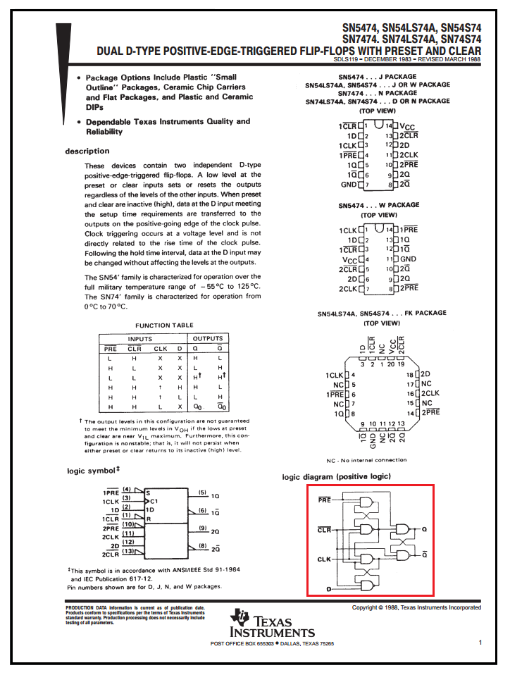
Here's how TI does it:

enter image description here

\$\endgroup\$
1
  • \$\begingroup\$ That's how TI did it in a design entirely different than a conventional master-slave flip-flop. The SN7474 uses three S-R latches and is not a master-slave design. If one is into such things, it is quite interesting to analyze the three S-R design and see how it works; it's much less obvious than a conventional master-slave FF. \$\endgroup\$
    – Eric Smith
    Commented Jul 21, 2017 at 6:35

Your Answer

By clicking “Post Your Answer”, you agree to our terms of service and acknowledge you have read our privacy policy.

Not the answer you're looking for? Browse other questions tagged or ask your own question.