I can't say I'm an expert in a computer architecture, but I'll take a shot at answering your questions.
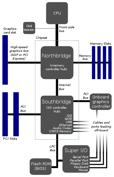
This looks to be the typical layout of motherboards.
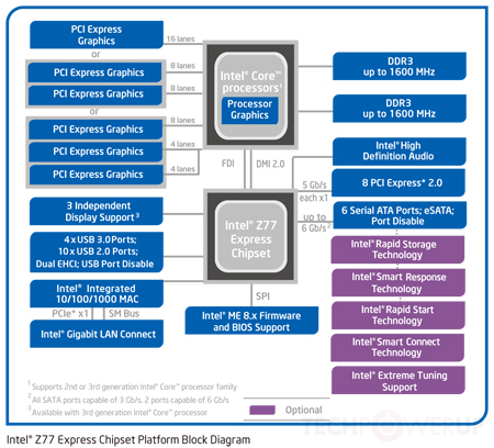
As Tom mentioned, this is no longer true. Most modern CPUs have an integrated northbridge. The southbridge is typically either integrated or made unnecessary by new architecture; Intel's chipsets "replace" the southbridge with the Platform Controller Hub, which communicates directly with the CPU via a DMI bus.
Why does the CPU connect to only 1 bus? That front-side bus looks like a major bottleneck. Wouldn't it be better to give 2 or 3 buses straight into the CPU?
Wide (64-bit) busses are expensive, they require a large number of bus transceivers and many I/O pins. The only devices that require a huge screaming fast bus are the graphics card and RAM. Everything else (SATA, PCI, USB, serial and so on) is comparatively slow, and not being constantly accessed. Hence why in the above architecture, all those "slower" peripherals are lumped together through the southbridge as a single bus device: the processor does not want to have to arbitrate every little bus transaction, so all the slow/infrequent bus transactions can be aggregated and managed by the southbridge, which then connects to the other peripherals at a much more leisurely speed.
Now, it's important to mention that when I say above that SATA/PCI/USB/serial are "slow", that's mainly a historical point, and is becoming less true today. With the adoption of SSDs over spinny disks and fast PCIe peripherals, as well as USB 3.0, Thunderbolt, and maybe 10G ethernet (soon), "slow" peripheral bandwidth is quickly becoming very significant. In the past, the bus between the northbridge and southbridge wasn't much of a bottle neck, but now that is no longer true. So yes, architectures are moving toward more buses attached directly to the CPU.
Is there something very hard about doing it this way? I don't see how cost could come into it, because the existing diagrams already have no less than seven buses.
It would be more buses for the processor to manage, and more processor silicon to deal with busses. Which is expensive. In the above diagram, not all buses are equal. The FSB is screaming fast, the LPC is not. Fast buses require fast silicon, slow buses don't, so if you can move slow buses from the CPU to another chip, it makes your life easier.
However, as mentioned above, with the increasing popularity of high bandwidth devices, more and more buses connect directly to the processor, particularly in SoC/more highly integrated architectures. By putting more and more controllers on the CPU die, very high bandwidth is easier to attain.
EDIT: I forgot to mention the Watchdog Monitor. I know I've seen it in some diagrams. Presumably a bottleneck bus would make it easier for the watchdog to monitor everything. Could that have something to do with it?
No, that's not really what a watchdog does. A watchdog is simply to restart various things when/if they lock up; it doesn't really look at everything moving across the bus (it's far less sophisticated than that!).


