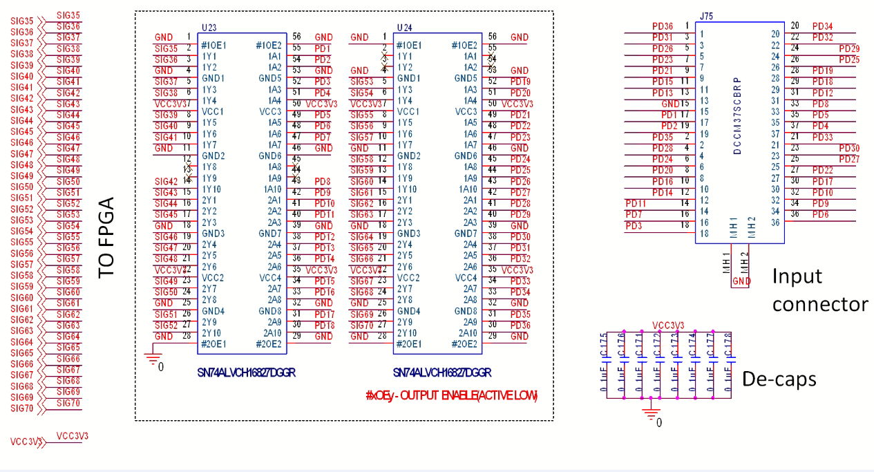
To buffer a LVTTL signal to FPGA I am using this TI buffer SN74ALVCH16827DGGR.The buffer IC is placed on a FMC based IO card mated to a ZYNQ mother card. The problem I am facing here is when an input signal is applied to the buffer IC, there is an output signal even when there is no power supply to this IC. The output enable signals are connected to PCB GND. I want to avoid this as it may damage the FPGA. Can someone suggest me with a solution?
-
\$\begingroup\$ Not a good idea. the ESD diodes are pulling Vdd up from the input which enables an output driven by your source. The 74ALC family has 25 Ohm driver. never apply signals before power on CMOS. this can cause latch up. \$\endgroup\$– D.A.S.Commented Mar 1, 2021 at 5:31
-
\$\begingroup\$ Is there any way I can use the same circuitry with some modifications and make the output low till the device is powered on. Or can you suggest me any other buffer IC which suits my application. \$\endgroup\$– saikumarkanikatlaCommented Mar 1, 2021 at 5:44
-
\$\begingroup\$ I don’t understand your interconnections but Pwr on reset low until Vdd detected. \$\endgroup\$– D.A.S.Commented Mar 1, 2021 at 5:48
-
\$\begingroup\$ You say that you are using this IC to 'buffer' the signal. Exactly why are you doing this? \$\endgroup\$– Bruce AbbottCommented Mar 1, 2021 at 7:12
-
\$\begingroup\$ Thank you @TonyStewartSunnyskyguyEE75 . But there are no IOs to control the POR. And I have made the output enable signals active default. \$\endgroup\$– saikumarkanikatlaCommented Mar 1, 2021 at 7:14
2 Answers
IC behaviour is usually unspecified when no power is supplied. As commented, you will try to power the whole board with your input signals in that case, due to the ESD protection diode.
There are, however special IC families that are are rated for this (for texas device look for the "Ioff partial power down" feature). Anyway I'd recommend at least a protection resistor on the inputs. Difficult to say more without the schematic.
-
\$\begingroup\$ Thank you. I have attached the snap of the schematic for reference. I havn't provided any series resistors on the input pins. \$\endgroup\$ Commented Mar 1, 2021 at 8:40
-
\$\begingroup\$ ALVC inputs do not have ESD diodes to Vcc and are overvoltage tolerant. Only at the outputs would an external voltage be a problem. \$\endgroup\$– CL.Commented Mar 1, 2021 at 10:26
-
\$\begingroup\$ @CL. Only at the outputs would an external voltage be a problem can you kindly explain this statement. \$\endgroup\$ Commented Mar 1, 2021 at 12:40
-
\$\begingroup\$ @lorenzo I want to use this IC SN74ALVTH162827 with Ioff = ±100 µA which has the same pin out of the IC I am currently using. Is Ioff = ±100 µA sufficient as I have 36 input signals to the board? \$\endgroup\$ Commented Mar 1, 2021 at 12:47
-
\$\begingroup\$ @saikumarkanikatla The inputs do not have ESD diodes to Vcc, but the outputs have them. So a voltage applied to an output (even when /OE is high) can allow a current to flow into Vcc, and thus power up the device. \$\endgroup\$– CL.Commented Mar 1, 2021 at 12:49
Thank you all for the support. SN74ALVTH16827 Solved my issue as it has Ioff feature, unlike SN74ALVCH16827.
-
1\$\begingroup\$ saikumarkanikatla - Hi, Thanks for coming back with this update. In order to mark the topic as solved, please consider "accepting" the answer which suggested that you look for the "Ioff" feature which you used (to accept an answer, click the "tick mark" next to your answer, to turn it green). Then the question is shown as having an accepted answer in various lists, and we don't get nagged for it being a question with an unaccepted answer. Thanks! \$\endgroup\$– SamGibson ♦Commented Apr 9, 2021 at 12:51

