Accepted answer to the question How are logic gates created electronically? can clarify most of your doubts. So I recommend you tor read that answer before reading this.
The basic steps involved in CMOS implementation are explained below taking NAND gate as an example. Hope that you can implement your logic following these steps.
Step 1: Write the inverted logic.
ie, if you want to implement Y, then write the expression for \$\overline{Y}\$.
For NAND gate,
$$Y=\overline{AB}$$ $$\overline{Y} = AB$$ So now Y should be low if
both inputs are high.
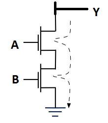
Step 2: Implement the NMOS logic (the pulldown network).
From output line, draw NMOS transistors (with inputs connected at its gate) to ground to implement the logic \$\overline{Y}\$. For and logic, connect in series and for or logic connect in parallel.
For NAND gate, \$\overline{Y} = AB\$, so draw two NMOS in series as
shown.

So now Y is low if both inputs are high.
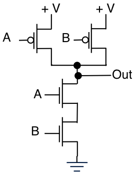
Step 3: Draw the dual of NMOS circuit to implement PMOS circuit (the pull up network).
ie, Replace each series connection with parallel and parallel with series connection. Implement the resulting circuit using PMOS and connect it from output line to Vdd.
The dual of AB is A+B. So connect two PMOS transistors in parallel
from Y to Vdd. 
So now out will be high if one of the inputs are high. This completes the logic.
