12
\$\begingroup\$

Using 2-ff synchronizers has been a standard for a signal to cross clock boundaries. And there are lots of paper/figures illustrating the mechanism, such as this one:enter image description here
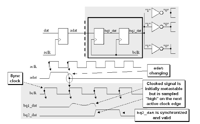
It seems bclk can only sample the pulse of adat once (at the second rising edge of bclk), which causes output metastability on bq1_dat. How can bq1_dat be sampled "high" on the next active clock edge?


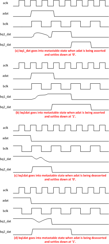
In addition to my question, I'd like to add what I think for a signal to go through safely to another clock domain (suppose 2-FF is enough to satisfy MTBF requirement). Please correct me if any mistakes.

enter image description here

ps: Metastable state does not display "wandering around" waveform, but a level that is neither '1' nor '0'. The following figure shows an example of metastable output. enter image description here
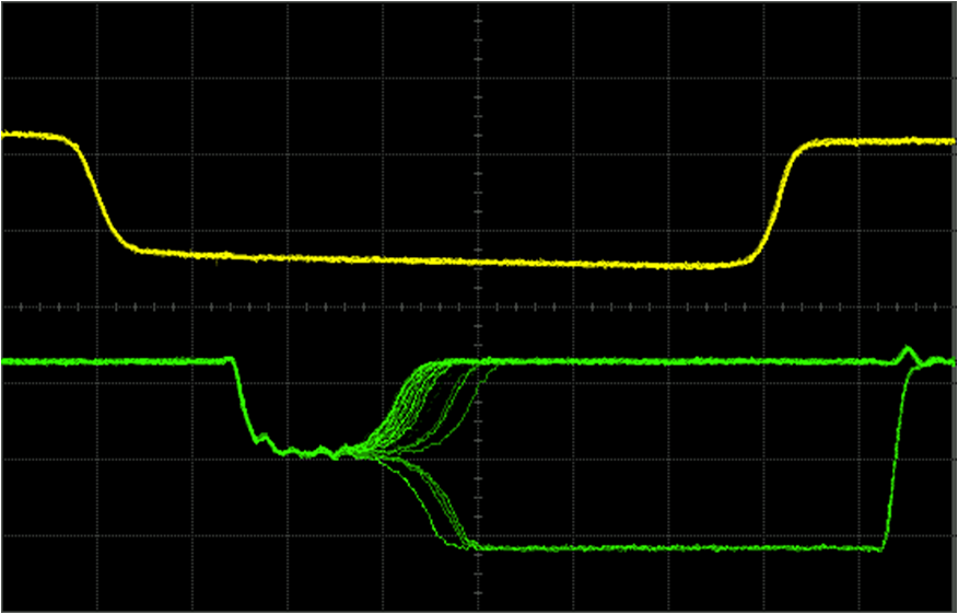
The original figure came from Lecture notes for EE108A, Lecture 13: Metastability and Synchronization Failure (ow When Good Flip-Flops go Bad) by W. J. Dally.

\$\endgroup\$
3
  • 4
    \$\begingroup\$ I just want to say that the diagrams that show the metastable output "wandering around" are extremely misleading. That isn't what metastability looks like at all. When a FF goes metastable, its output goes to a single, specific intermediate voltage (the value depends on the implementation technology) and stays there. After some unpredictable amount of time, the voltage will then swing either high or low, and which way it goes is also unpredictable. \$\endgroup\$
    – Dave Tweed
    Commented Jun 3, 2016 at 11:26
  • 1
    \$\begingroup\$ @Dave Tweed♦ Thank you for the comment. In almost all the documents I've read concerning metastability, I saw the "wandering around" waveforms. I searched around and found a post (If a flip flop has a setup violation and goes metastable, is it guaranteed to settle to the input value when it finishes oscillating?) containing a shoot from o-scope with metastable state captured. A link to the original reference of the figure is included in that post. \$\endgroup\$
    – fiedel
    Commented Jun 6, 2016 at 1:48
  • \$\begingroup\$ Yes, that illustrates my point perfectly, and the Powerpoint presentation it comes from has a lot of good information in it. \$\endgroup\$
    – Dave Tweed
    Commented Jun 6, 2016 at 2:32

2 Answers 2

10
\$\begingroup\$

The simple answer is that they don't on their own. The synchroniser is there not to ensure the data gets across, but the ensure you don't end up with metastable signals feeding lots of other signals and causing problems. The second FF as the diagram shows catches the metastable first FF output and prevents it propagating further through the design.

There are various sorts of signals, and how you include synchronisers depends on what signal you are talking about. But lets look at a couple of common types:

  1. Trigger Signals - or any signal which is basically a pulse which must start something else running. These generally carry no data, and all you are interested in is that there is, say, a rising edge in order to start something going in another clock domain. To get these to cross over, you would need a synchroniser (essentially doing what is shown in your diagram), but you need a little bit more.

    The simplest option is to extend the pulse - essentially you make sure the input pulse is more than 1 clock periods of the destination clock (it should be longer than 1 cycle by at least the larger of the setup and hold times for the destination register). For example if you are going from a 20MHz clock to a 15MHz clock, you would make sure your pulse is two clock cycles at the input which would ensure that it is presented to the destination clock and not lost. This also answers your question in how the signal is guaranteed to go across. If the pulse is wider than one destination clock period it means that if it goes metastable on the first clock edge and ends up being seen as a 0, then on the second clock edge it will definitely catch the pulse.

    Because with this type of signal you are only interested that the pulse has gotten across, it doesn't matter if the output signal ends up with two clock cycles high some of the time and only one cycle the rest. If you need to ensure it is a single cycle pulse, you can instantiate a simple edge detector circuit.

  2. Control Buses - or possibly types of data buses. These are arguably more difficult because if you have multi-bit data stream that needs to stay synchronised. In this case what you would do is implement something called "handshaking". You basically load your data on the source clock and hold it. Then you send a request signal (like in 1) across through a synchroniser. Once the request signal is across you know that the data bus will also be stabilised in the destination domain. You can then clock it into a register bank in the destination. The destination then sends an acknowledge pulse back again to inform the source that it can load the next word.

    You would use this sort of bus if you needed to send a control word to the destination clock for which you need to know that it has gotten there before you send another (e.g. if you are sending a command to do something).

  3. Data buses - for data where you have a source that spits out data continuously or in bursts, you are arguably better off using a FIFO than synchronisers. The FIFO uses a dual-clock memory to hold the data, along with counters to keep track of how much data is in the FIFO. You write the data in to the FIFO when there is space, and then increment the write address. This address is then typically encoded into a "Gray Coding" scheme which ensures that each increment in address causes only one bit in the address bus to change (meaning you don't need to synchronise multiple bits). This address is then transferred to the destination domain (through one of your synchroniser chains), where it is compared with the read address. If there is data in the FIFO, it can then be read out of the memory using the destination clock port. The read address is similarly Gray coded and sent back to the source through another synchroniser so that the write port can calculate if there is any space in the FIFO.

  4. Reset Signals - these typically use a modified version of the synchroniser in what is know as "Asynchronous Assert, Synchronous Deassert". In this modifed version, the data input to the first flip flop is tied to GND, and instead the incoming reset signal is connected to asynchronous preset signals of each flip-flop in the synchroniser. This results in an output signal which is entirely asynchronous when it goes high, but the synchroniser chain ensures that it goes low synchronously with the destination clock by clocking through zeros in the register chain.

    This type of synchroniser is terrible for data and control, but perfectly suited to reset signals. If all the destination logic feeds the output of this chain into the asynchronous reset inputs of any register in the domain, then there is little worry of metastability on assert (even though it is asynchronous) as all the registers are forced to a known state. Then when the reset signal is deasserted in the source domain, it synchronously deasserts in the destination domain meaning all registers come out of reset on the same clock cycle (rather than +/- 1 cycle if it was asynchronous deassert).


As you can see from the above, it is a lot more complex to do clock-domain crossing than to just stick a 2 flip-flop synchroniser on the signal. The exact method used depends on the application.

\$\endgroup\$
5
  • \$\begingroup\$ In addition to Tom's answer, I like to add a reference to PoC, which has implementations for these cases. The synchronizer docs are available on RTD. Additional to the theory of chaining 2 flip-flops for a basic 2-FF synchronizer, PoC provides dedicated implementations (sync_Bits) for Xilinx and Altera FPGAs to improve the metastability behavior. The 2-FF synchronizer is used for example in sync_Strobe to build more complex synchronizers for pulses. \$\endgroup\$
    – Paebbels
    Commented Jun 2, 2016 at 7:26
  • \$\begingroup\$ Thank you for the elaborated introduction to synchronization strategies. This picture came from "Clock domain crossing (CDC) design & verification techniques using systemverilog" by Clifford E. Cummings. I understand that for a one-bit signal, the width has to be at least 1 clock cycle +setup time+hold time of the receiving side for it to get through safely. In this picture, this criteria is not satisfied as the pulse of adat is sampled by bclk samples only once on its falling edge, which causes bq1_dat to be metastable. \$\endgroup\$
    – fiedel
    Commented Jun 3, 2016 at 3:27
  • \$\begingroup\$ ... As a result, the reading of bq1_dat at the next rising edge of bclk could be either '0' or '1'. So the synchronization in the picture seems to be unsuccessful. Am I right? \$\endgroup\$
    – fiedel
    Commented Jun 3, 2016 at 3:27
  • \$\begingroup\$ @Paebbels Thank you for the reference. Will take a look =) \$\endgroup\$
    – fiedel
    Commented Jun 3, 2016 at 3:29
  • \$\begingroup\$ You should edit this into your question, not post it as an answer, but essentially, yes, you may or may not get a 1 at the output in that example. \$\endgroup\$ Commented Jun 3, 2016 at 3:56
1
\$\begingroup\$

1) Using your drawing as an example, aclk and bclk are asynchronous to each other. In other words, they have different clock sources. They are showing adat as valid data but synchronized to aclk only. This is where the bclk synchronizer comes into play.

2) This drawing assumes a worst-case scenario, where bq1_dat is a messy output because the bq1 FF caught only part of the end of the data, creating a metastable state upon which the output is usually garbage. Here's the trick. Bq2 has the same bclk as bq1, but it takes 2 clock cycles of bclk for data to pass through and appear at bq2_dat.

3) The first bclk captured part of the data, resulting in a messy output, but the second bclk is one clock cycle later, enough time for ambiguous data from bq1_dat to settle into a high or low state. The messy bq1_dat pulse lasted just long enough for bq2 to capture a valid logic '1' (logic high), and pass it to bq2_dat as valid and now synchronized data (logic high).

4) Downstream, any clock using bclk will have synchronized data to work with. Notice that only the first bclk FF had to deal with a metastable state. The output could have been a logic low if adat had been just pico or nano seconds too late. Remember these flip-flops sample the data input only on the rising edge of the clock. What happens before or after the rising edge is ignored.

\$\endgroup\$
5
  • \$\begingroup\$ Note though, that the bclk delay only provides a probabilistic measure of safety, and the exact amount depends both on the FF technology and the bclk period. In some hi-rel cases 3 or even more stages may be required to get the error rate down to acceptable levels. \$\endgroup\$ Commented Jun 2, 2016 at 3:57
  • \$\begingroup\$ @WhatRoughBeast. I know that in worst case scenario's many sync stages are needed, plus digital filtering. Obviously my answer was too simple. \$\endgroup\$
    – user105652
    Commented Jun 2, 2016 at 19:20
  • \$\begingroup\$ @Sparky256 What puzzles me is 3) in your comment. How can bq2 capture a '1' when bq1_dat is in metastable state? \$\endgroup\$
    – fiedel
    Commented Jun 3, 2016 at 3:32
  • \$\begingroup\$ @fiedel, two things contribute to bq2 being able to capture a clean input (at least). First the metastable state needs to persist for a full clock cycle. Second, the metastable (pseudo-mid-rail) value from bq1 could be unlikely (or optimised to avoid) to be in the window that would also cause bq2 to be metastable - but its mainly the first of these. Say the technology results in 5% chance of metastability persisting long enough. a 3-FF sync stage would reduce this to 0.25% because both cells have to fail. Messy is in practice a well-defined exponential deviation from the nearly-stable state. \$\endgroup\$ Commented Jun 3, 2016 at 11:58
  • \$\begingroup\$ @SeanHoulihane. Thanks for the explanation. The term 'rising edge' confuses some because the window of accepting data (metastable or stable) is at the halfway point of the rising edge, lasting a few pico or nano seconds only. Only at that instant is the input data at a logic '1' or '0', whether it is metastable or stable, depending on its voltage level compared to the IC's threshold for logic 1 or 0. \$\endgroup\$
    – user105652
    Commented Jun 3, 2016 at 19:42

Your Answer

By clicking “Post Your Answer”, you agree to our terms of service and acknowledge you have read our privacy policy.

Not the answer you're looking for? Browse other questions tagged or ask your own question.