9
\$\begingroup\$

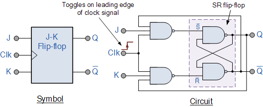
My background is in Computer Science, and this is my first time posting in electronics SE. This is a circuit diagram of JK flip flop.

Circuit diagram of flip flop

I don't understand how it works at the beginning, when the circuit is first on. In my understanding, Q and Q' does not have a value yet, then how does the circuit proceed? I was reading from this website. I have tried three more websites, yet did not find the explanation.

\$\endgroup\$
10
  • 2
    \$\begingroup\$ Usually there is a reset/preset/clear signal to flops which you assert to set the flip-flop output to 0 or 1 initially + you don't tie JK inputs as floating. It should be either 0 or 1 always and start analysing from that point. \$\endgroup\$
    – Mitu Raj
    Commented Dec 1, 2020 at 5:30
  • 1
    \$\begingroup\$ It actually makes a lot of sense but what does "you don't tie JK inputs as floating" mean? \$\endgroup\$
    – alu
    Commented Dec 1, 2020 at 6:34
  • 1
    \$\begingroup\$ Floating means like "not connected to anything". You either feeds 0 or 1 to the inputs always. \$\endgroup\$
    – Mitu Raj
    Commented Dec 1, 2020 at 7:11
  • 4
    \$\begingroup\$ @MituRaj The inputs don't need to be floating to make the initial state undefined. Consider the case with all inputs tied to 0. \$\endgroup\$
    – Sneftel
    Commented Dec 1, 2020 at 9:28
  • 3
    \$\begingroup\$ The logic diagram is bad. This is a JK latch, not a real clocked flip-flop. It has a hazard when J and K are both ‘1’ and the clock is high. See my answer. \$\endgroup\$ Commented Dec 1, 2020 at 16:39

3 Answers 3

12
\$\begingroup\$

The JK flop can power up in either state. With perfectly matched gates, the odds would be 50-50 for each state. It is up to the rest of the system to initialize to a known, desired state, or to not care about it. Same goes for a D flop.

It’s the same as having an uninitialized variable in a program. Until the variable is set, any values that depend on it (including itself) are not known.

Hardware simulation of this flop would show up as an ‘X’ state until it has had a 0 or 1 clocked into it. Otherwise, it will stay ‘X’ if both J and K are 0 (hold) or 1 (toggle).

In actual hardware (like software), unknown things could happen depending on how the unknown-state output is used.

A variant of this flop has direct set and clear inputs to force an initial state with separate signals (e.g., reset.) In that case a startup behavior can be defined.

MORE: the logic diagram shown for the JK is crap. This is actually a gated JK latch, and it has a hazard when both J and K inputs are ‘1’ and the clock is high: it becomes a ring oscillator due to the 'race around' issue.

Unfortunately, while the the linked article discusses this, it gives a mealy-mouthed answer about using a very narrow clock pulse to avoid the ‘race around’ issue. This is hugely misleading. Integrated circuit-based JK flops use a pair of latches wired as 2 stages ("master-slave" or "edge-triggered") and don't have the race-around problem.

Another complaint. The logic diagram given for the 74xx73 type JK is not only incomplete (doesn't show set/reset), it's wrong (74xx73 uses the 2-latch "master-slave" design, not gated latch.) I left a note for the page author for them to fix it.

This answer discusses the JK gated-latch problem in detail. SR FlipFlop Question

And here: JK latch, possible Ben Eater error?

\$\endgroup\$
6
  • \$\begingroup\$ This has a lot of information but my confusion is: Say at the beginning J=0 and K=1. So the J NAND gate would output 1, since any of the inputs zero implies the result would be 1. Now this 1 goes to the S' NAND gate, but since it is 1, we don't know what the result would be. Then if we go back to the K NAND gate, we can't know what the output would be, since if one input is 1, the output relies on the rest of the inputs. So how would the operation proceed from there? \$\endgroup\$
    – alu
    Commented Dec 1, 2020 at 6:30
  • 2
    \$\begingroup\$ You're right. You don't know what the output would be. It's in a random state (could be 1, could be 0) until the flip-flop is reset or a known logic value is clocked in. If there are devices further down the line from the flip flop which depend on it's value, they too will be in a random state. I think what you're missing, when you say "At the beginning J=0 and K=1" then talk about how S' and R' feed back. But you don't mention the state of the clock. That's a 3rd input to the Nand gate Consider your setup when the clock =0, then what happens when the clock changes to "1"?? \$\endgroup\$
    – Kyle B
    Commented Dec 1, 2020 at 8:36
  • \$\begingroup\$ @alu, your concerns are valid. We can fix this by using an asynchronous input which sets the output to a known state. \$\endgroup\$ Commented Dec 1, 2020 at 10:40
  • 1
    \$\begingroup\$ The diagram shown is a JK latch with a hazard. Added this to the answer. \$\endgroup\$ Commented Dec 1, 2020 at 16:41
  • \$\begingroup\$ I read the answers multiple times, including the linked ones. I understand a little bit now but it's not clear. Mainly when I imagine physical circuit and it depending on the rest of the system, I imagine it works in a manner that I won't understand. And I understand initially when the circuit powers up, all of the gates including Q and Q' get some voltage somehow, possibly like John Doty said, and then they reach some state which makes the circuit working as desired. That's all I understand for now, and I am tired from trying to understand without any progress. \$\endgroup\$
    – alu
    Commented Dec 4, 2020 at 6:52
10
\$\begingroup\$

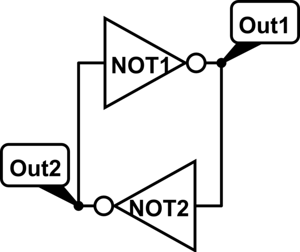
When power first comes on, this can't be understood as a digital circuit. To the actual physical circuit, inputs and outputs can be between 1 and 0, or even beyond. Part of designing logic primitives is hiding this from higher level design, but it's a "leaky abstraction". Consider the following simple example:

schematic

simulate this circuit – Schematic created using CircuitLab

Now, plainly, as a digital circuit, if Out1 is 0, Out2 is 1, or vice-versa, forever. So, what happens on power-up?

Imagine that on power-up, both Out1 and Out2 are 0. In that state, Not1 and Not2 will slew their outputs toward 1. But somewhere in between 0 and 1, they'll switch, driving back toward 0. Now, the circuit is never built in perfect balance, and thermal noise is also present, randomly influencing this process. So, one of the two inverters switches output polarity before the other one and wins the race to 1. That drives the other to zero. The circuit may briefly thrash around, not behaving as nice Boolean logic, but it quickly settles into a well-defined logic state. With a real circuit, you generally get biased random behavior: one state is favored over the other, but there is some randomness.

\$\endgroup\$
2
  • 2
    \$\begingroup\$ This is actually a beautiful description \$\endgroup\$
    – alu
    Commented Dec 2, 2020 at 7:00
  • \$\begingroup\$ I don't understand how NOT gates race for 1. I assume they try to reach a certain voltage but gets interrupted by the other one. Now I don't know how that works in a real circuit, I imagine it will take a lot more effort to understand. \$\endgroup\$
    – alu
    Commented Dec 4, 2020 at 6:57
2
\$\begingroup\$

Q and Q' does not have a value yet, then how does the circuit proceed?

That is correct. There is no way to know how the circuit would proceed.

To fix this we can use an asynchronous or synchronous RESET or PRESET input to set the output to a known state. An asynchronous input does not depend on the clock, but a synchronous input depends on the clock.

Here is a reference circuit for a Master-Slave JK Flip-Flop with asynchronous reset and set inputs.

JK Flip-Flop with Asynchronous RESET and SET input
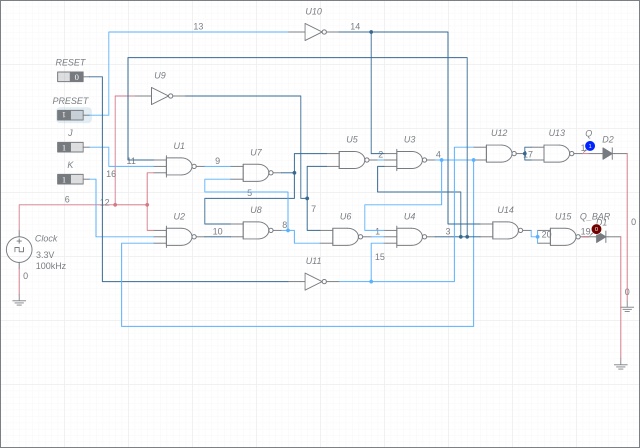
JK Flip-Flop with Asynchronous RESET and SET input simulate this circuit - Schematic created using MultisimLive

This is the circuit of a JK Flip-Flop with an asynchronous RESET and PRESET. A HIGH on an asynchronous RESET input sets Q to LOW and Q' to HIGH, and this operation is independent of the clock. Similarly, a HIGH on an asynchronous PRESET input sets Q to HIGH and Q' to LOW.

Working:

When the RESET input is HIGH, the output of the NOT gate (U11) will be LOW. The output of the NAND gate (U12) will become HIGH since one of the inputs is LOW. This will make the output of the NAND gate (U13) Q to be set to LOW. Similarly, other cases can be analysed, and is left as an exercise to the reader.

Note:

Behaviour is not defined for the case when both PRESET and RESET are HIGH, since it is not allowed (and meaningless).

Further reading

The section 2 of this paper by Clifford Cummings, Don Mills and Steve Golson is particularly relevant, so I'm quoting it here

For individual ASICs, the primary purpose of a reset is to force the ASIC design into a known state for simulation. Once the ASIC is built, the need for the ASIC to have reset applied is determined by the system, the application of the ASIC, and the design of the ASIC. For instance, many data path communication ASICs are designed to synchronize to an input data stream, process the data, and then output it. If sync is ever lost, the ASIC goes through a routine to re-acquire sync. If this type of ASIC is designed correctly, such that all unused states point to the “start acquiring sync” state, it can function properly in a system without ever being reset. A system reset would be required on power up for such an ASIC if the state machines in the ASIC took advantage of “don’t care” logic reduction during the synthesis phase.

We believe that, in general, every flip-flop in an ASIC should be resetable whether or not it is required by the system. In some cases, when pipelined flip-flops (shift register flip-flops) are used in high speed applications, reset might be eliminated from some flip-flops to achieve higher performance designs. This type of environment requires a predetermined number of clocks during the reset active period to put the ASIC into a known state.

ASIC: Application Specific Integrated Circuit

\$\endgroup\$
2
  • 1
    \$\begingroup\$ How to use asynchronous RESET? How does it work? \$\endgroup\$
    – alu
    Commented Dec 2, 2020 at 7:00
  • 1
    \$\begingroup\$ @alu, good question. I've added a circuit to my answer which you can now simulate in your browser. I've also added the working of my design. \$\endgroup\$ Commented Dec 2, 2020 at 9:44

Your Answer

By clicking “Post Your Answer”, you agree to our terms of service and acknowledge you have read our privacy policy.

Not the answer you're looking for? Browse other questions tagged or ask your own question.