You've received some good answers and I agree that the currently selected best answer should be the best answer, but I wanted to add some insight.
When we call an undriven node "floating" we do it for one very good reason. Electrical nodes (wires) capacitively and inductively couple charge from all over the place. The basic principle is why motors and generators do what they do: charge is coupled between the rotor and stator windings. In motors and generators, this is desirable. In the world of microelectronics, we call this undesirable effect crosstalk.
Crosstalk is coupled from everywhere: other nearby nodes including signal nodes (wires used to transmit data) and clock nodes (evil little badgers when it comes to crosstalk), the power plane, the ground plane, and the substrate. Capacitive and inductive modeling for very high speed signal paths is detailed (bordering on enormous) literally for this one reason alone. Not-cutting-edge designs often only focus on the capacitive element because the wire lengths aren't long enough for the inductive element to matter as much and, as a result, simulation time is greatly reduced. Really-not-cutting-edge designs often lump capacitances together to further speed up the simulations.
My point is, without doing something to guarantee a signal node will be driven high AND low, the node's voltage will bounce all over the place. In the designs I worked on, it wasn't uncommon for the voltage to jiggle around 75% of Vcc simply because no insulator (including your substrate) is perfect. This is a frankly massive problem as the 75% transition point is usually within the metastable region of CMOS operation (the region where the circuit doesn't quite know whether it wants to be high or low, meaning it's moderately resistive and sensitive to crosstalk).
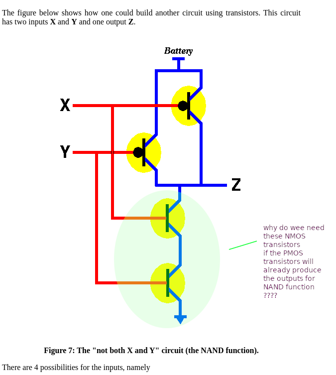
For completeness, consider that one pair or the other of your MOS transistors can be replaced with a single resistor (depending on which pair you pick, connected to Vcc or Gnd). This will work great so long as the ratio between the MOS on-resistance and the resistor is enough to allow the signal voltage to clear the gate-off voltage, but it will be power-hungry and slow. (In some of my old designs a very small NMOS transistor would be gate-to-drain connected to make it a resistive diode. We'd use this in reset circuits where the occasional pulse to reset something was so rare that the higher power loss and slower speed weren't an issue compared to the space savings of a full CMOS setup.)
My own background (from 30 years ago) was (is...) in BiCMOS design. Conceptually, a simple inverter was a 3-inverter device. The first CMOS inverter was very small. It drove a larger CMOS inverter, which then drove a Bipolar transistor array that had very, very small parallel CMOS devices. The result was a device that could drive an enormous amount of energy. (Usually data backplanes.) The technology was spectacularly good for 1V solutions on satellites.
But if you think about it, that means you have the traditional diode voltage drop. That's why we used the parallel CMOS devices, to guarantee full transition rather than a partial transition.
To summarize, when designing in a digital world, you want (a) full control over every data node and (b) as much control over capacitive and inductive coupling as possible. (A) is more important than (b) because you can't completely control (b).


