Problem:
We design a PCB with an JTAG compatible FPGA that I need to program.
Now I want to be able to access the JTAG Interface from either a connector (_A) or an FT2232H USB controller (_B).
The main interface would be FTDI Device while the connector should act as Backup if progamming from FTDI fails for some reason.
Question:
What is a proper way to split the signals between the connector and the USB Chip ? Or do i need to split them at all ?
I have 2 ideas so far. Maybe someone has a better idea for this ?
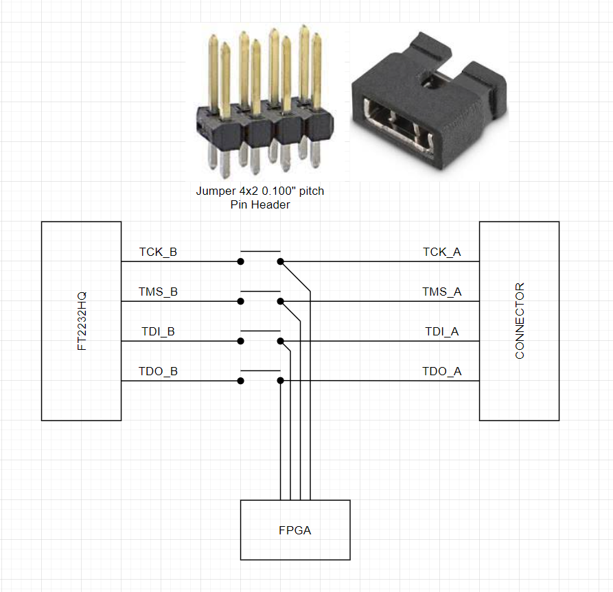
IDEA 1
Will this add noise or any significant quality loss to the signals ?
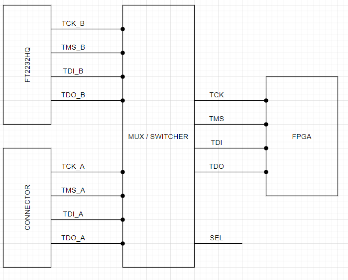
IDEA 2
Looks like an elegant way to do it. My only concern is that the MUX will pull the signals that are not connected to ground via 6M Ohm internal pull down resistors (from Datasheet of the Mux). Does this affects the FTDI chip in any way ?
Thanks in advance


