6
\$\begingroup\$

Assume a x16 DDR SDRAM module with 2b banks, which are made of 2r rows, which are further composed of 2c columns, where each column is 2w bits "tall". Assume that the interface is burst-oriented, with a burst length of 2bl. I.e. one data transfer consists of one 2(w+bl)-bit data packets. Each row must then be 2(c+w) bits wide.

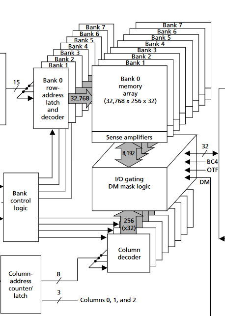
As I understand it, each bank has a separate set of 2(c+w) sense amplifiers. Upon bank activation, the entire selected row is "transferred" into the sense amps. From there, a column decoder selects the 2(w+bl) bits that will either be read from or written to. I am drawing these conclusions from a DDR3 SDRAM block diagram, for example this one from a Micron datasheet, for a x16 device with 214 rows and 210 columns.

enter image description here

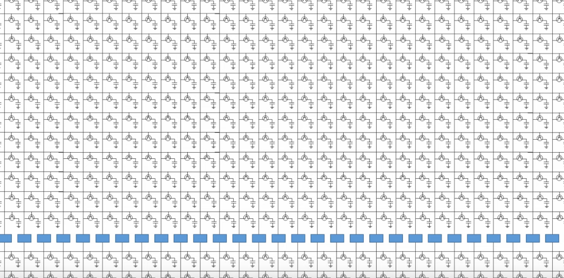
Each bank, then, is composed of 2(r+c+w) memory cells, which are divided into two groups by the 2(c+w) sense amplifiers, like so (the blue rectangles being the sense amps)(image source is this youtube video):

enter image description here

It stands to reason, then, that there are 2(r-1) cells above each sense amp, and 2(r-1) cells below each sense amp, for a total of 2(r). This way, each address line within the memory array addresses one entire row.

The problem in my theory here is that the sense amp is (supposedly) also used as a refresh circuit. In DDR3, there are 8192 refresh cycles, one every 7.8 us, as each capacitor can only hold charge for 64 ms. If a refresh is effectively just a read, then how are the memory cells (of, say, 2^14 rows and 2^10 columns, each 16-bit wide) divided into 8192 groups?

I've seen a ton of articles and papers and videos discuss this topology, but the naming of "row" and "column" in literature is confusing and not uniform. I believe I've come to a plausible solution, but I must still ask: Is my understanding correct?

\$\endgroup\$

1 Answer 1

1
\$\begingroup\$

A few corrections:

  1. Technically DDR columns have "width" not "tall" which is basically the x16 in your case i.e 16 bit wide.
  2. Burst length is directly tied to prefetch number which is a jedec spec of 2n, 4n or 8n. Which is basically telling if we are accessing 32 or 64 bit in the DDR config. It is not necessarily a power of two. It is more like how many columns are needed to make a proper DDR word.

Now for the explanation:

The storage cells themselves are activated using differential lines and its not a straight interface to the row line. The address is demuxed to rows and column demux logic modules which then activates a group of differential lines which put the sense amplifier as well as the cell on the same differential bit lines allowing the sense amp to basically amplify the weak charge in the cell to an actual logic voltage. This process actually destroys the data in the D-RAM cell and hence the sense amp also does a restore of the data by writing it back. The term "sene amp" here refers to the entire circuitry that gates the bit and not just the differential amplifier.

In the example:

  1. Each bank has 215 (32Kib) cells in total.
  2. Each bank has 32ki rows.
  3. Each row has 256 x 32 = 8192 cells.
  4. Each column is 16 bit wide here. The pre-fetch is 2n (DDR1 standard) which means two 16 bit columns are read for a total of 32 bits. You can see that in the I/O gating output line marking.
  5. Each row has 256 columns of 32 bit words (4bytes).
  6. 3276825632*8 = 2Gib is density of the chip with a configuration of 128M x 16.

When you give bank x row x column address, you are basically reading 32 bit data as you should with a legacy system using DDR1 on a 32 bit cpu. What happens then is that the 32 bits are stored into two 16 bit prefetch buffers and send over the data line in two burst transfers of 16 bit each i.e DQ[0:16].

DDR spec did mention of 64 bit wide data using x32 interfaces. There is very little info on that but it's a logical expansion of the data size.

The term 'row' and 'column' refer to the logical arrangements of the cells in a bank. each decoded address corresponds to a row.

You start with chip density = D Total cells in bank Cb = chip density / number of banks

r bit address => 2r rows

Each row has Cr cells which should be same as Cb / 2r

If cell width is Cw and prefetch is Pn then number of cells per row is: Cr / (Pn x Cw)

If you see the diagram in your question, these numbers are already given at appropriate locations, You don't need to calculate anything.

\$\endgroup\$

Your Answer

By clicking “Post Your Answer”, you agree to our terms of service and acknowledge you have read our privacy policy.

Not the answer you're looking for? Browse other questions tagged or ask your own question.