3
\$\begingroup\$

I'm trying to understand this D type positive edge flip-flop:
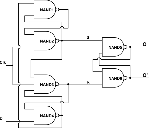
schematic

simulate this circuit – Schematic created using CircuitLab

I'm having problem understanding why it is positive edge triggered and not level triggered.

I understand that when the clock is 0, NAND 2 and 3 will both output 1 locking the current values of the SR latch on the right.

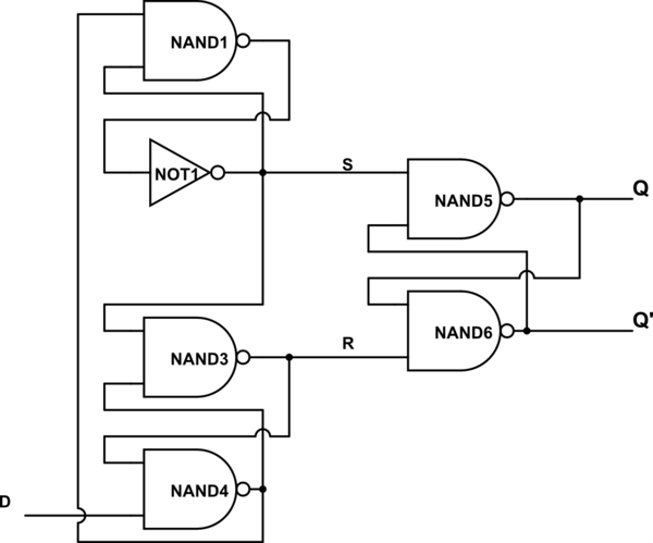
When the clock value is 1, it stops affecting the circuit so it can be simplified into something like:
schematic

simulate this circuit

Where the circuit will start to be affected by the input of D according to the previous state of the circuit.

If this is how this D type flip flop works, wouldn't it be a level triggered flip flop instead? The input D will affect the set and reset values of the SR latch on the right as long as the clock is 1.

Can someone explain where I've gone wrong in my understanding?

\$\endgroup\$
3
  • \$\begingroup\$ It is a good question. I found this Why edge triggering is preferred over level triggering? \$\endgroup\$
    – user34299
    Commented Dec 12, 2015 at 17:10
  • \$\begingroup\$ Thanks for the reply, i've read the link you provided, but it doesn't really answer my question, it just explains why edge trigger is more precise. After reading it, I still don't understand how this DFF is considered edge triggered, since edge trigger would be the output values can only be affected when the clock is on an edge; but from my understanding, this DFF output is affected whenever the clock is on the level 1 \$\endgroup\$
    – Victor Lin
    Commented Dec 12, 2015 at 17:20
  • \$\begingroup\$ No it is not, it keeps the state it was in at the moment that the clock became 1 (as it is supposed to). Note that NAND1 and NOT1 form a memory and so do NAND3 and 4. When S = 1 R must be 0 so NAND4 will ignore D. When R = 1 NAND3 and 4 cannot change state as as S = 0. R and S cannot be both 1 at the same time. \$\endgroup\$ Commented Dec 12, 2015 at 18:47

2 Answers 2

5
\$\begingroup\$

No, your circuit is still a edge-triggered circuit. The pairs NAND1+NAND2 and NAND3+NAND4 lock the state of D when the clock rises from to low to high. Changing D when the clock is high (after the rising edge) does not affect the output.

Let's start with Clk = 0, then is S=1 and R=1.

Now let D=0 during the rising edge of the clock:

  • The output of NAND4 will be high.
  • The output of NAND3 will be low, because S is still high, thus R=0 => Q=0.
  • The output of NAND1 is low.
  • The output of NAND2 is high, thus S is high, and R keeps low.

The output of NAND4 will be kept high until the clock is low again because the input connected to R is low regardless of any change on D (after the rising edge).

Please note that the functionality of this circuit relies on the propagation delay of the gates.

\$\endgroup\$
1
  • \$\begingroup\$ Ah, thanks for your explanation, that sure cleared up my confusion. Basically NAND 3 will act as lock when D=0 by outputting 0 into NAND4, and NAND 2 will act as lock when D=1 by outputting 0 into NAND1. \$\endgroup\$
    – Victor Lin
    Commented Dec 13, 2015 at 3:51
0
\$\begingroup\$

If the circuit is a 7474 D - Edge triggered, unless I am wrong, you are not really "wrong".

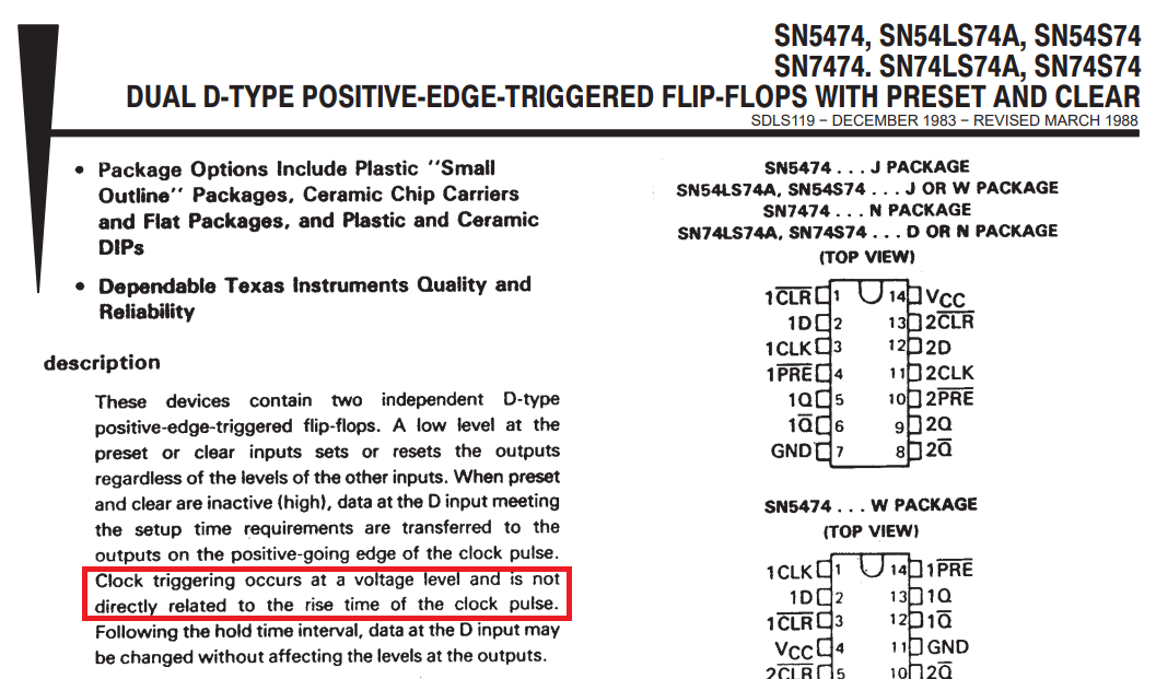
From the datasheet https://www.ti.com/lit/ds/symlink/sn54ls74a-sp.pdf?ts=1629843026340&ref_url=https%253A%252F%252Fwww.google.it%252F

See the description

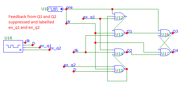
For proving this, one must use a "variable slew-rate" clock.

enter image description here

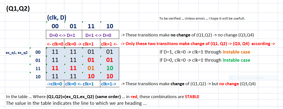
EDIT: to prove that it is really the transition 0 to 1 of the clock that is meaningful, I will add the excitation kmap of the first two RS latches. The behavior of the last (at right) is straightforward. Here is the circuit with feedbacks removed. Kmap coming soon ...

enter image description here

For each change of the input values of (clk, D), follow the values in the map.
Remember that in this map, one only can move horizontally (under change of clk or D, only one at one time), then move vertically until a stable combination is found ... if any ...).
The "state" in the "box" show to what "line" we are heading (shown at the left of the table) ... Continue until we are in a RED case, which is "stable" combination if any.

enter image description here

\$\endgroup\$
2
  • 2
    \$\begingroup\$ No, I don't think this sentence in the datasheet means that the 7474 is level sensitive. The "voltage level" mentioned here is not a logic '0' nor a logic '1', it is some voltage in between. The sentence is saying that the FF will change state when the clock passes through that "voltage level", it does not say that you can hold the clock at some specific voltage level and changes on the input will fall through to the output. \$\endgroup\$ Commented Aug 25, 2021 at 15:41
  • \$\begingroup\$ Yes. Sensitive at "one level" between "0" and "1", but not "0" or "1". Just the "change" "0" to "1" is meaningfull. Ok. \$\endgroup\$
    – Antonio51
    Commented Aug 26, 2021 at 5:35

Your Answer

By clicking “Post Your Answer”, you agree to our terms of service and acknowledge you have read our privacy policy.

Not the answer you're looking for? Browse other questions tagged or ask your own question.