I'm (still) a relative beginner in PCB layout. I'm trying to understand in what scenarios it's important to route with polygon areas instead of traces, and in those scenarios, just how important it really is - and why. X/Y disclaimer: the motivation for my question is that the tool I currently use, EAGLE, isn't great at polygons - it's quite a pain: it takes more time, is much more fragile, and I want to learn if and when I can or even should be lazy and use traces.
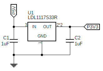
Consider the following simple layout problem: an LDO (LDL1117) in a SOT-223-4 package with input and output capacitors:
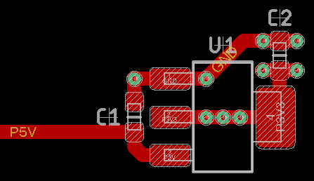
Let's assume a 4-layer board with GND and 3.3 V planes to which we can drop with vias. I would route this as follows (please feel free to critique - I am open to learning):
(Later I'd also pour GND on the top layer, which would "wash out" the GND trace from U1.1 to C2.)
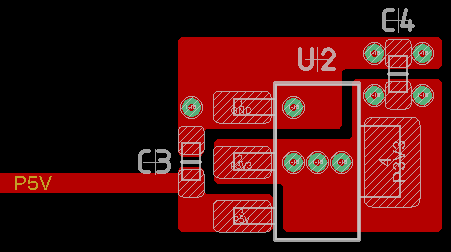
But when I look at "professional" designs, I more often see something like this (again, critique welcome):
I can think of the following pros/cons:
- Higher current-carrying capacity with the polygon areas with less temperature rise.
- For higher frequency signals, lower loop area since the current has more area available to seek the lowest-impedance path.
- Solderability - I think the polygon areas will increase heat sinking and make it harder to hand-solder (more heat required). I'm not sure if there is any impact with professional reflow / wave soldering processes.
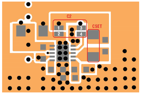
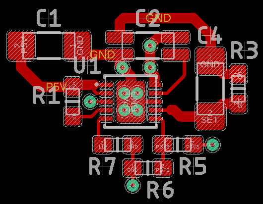
Let's look at a more complex example, this time using the ultra-low-noise, ultra-high-PSRR LT3024 LDO. The evaluation board has the following layout1:
I can reproduce this in EAGLE, but it's such a pain that I find myself wishing I could just do this2 instead (this is my mockup, and my reference designators match those of the evaluation board):
So just how much am I sacrificing if I choose to be lazy and use traces instead of polygons? If I have a relatively low-frequency, low-current (< 200 mA in the LT3024 example) circuit, does it really matter? Why, or why not?
1 I've studied the datasheet and evaluation board extensively, and I'm aware of the "special techniques" recommended, such as Kelvin-connecting the output capacitor and stacking the input + and - traces to cancel EMI when post-regulating DC/DCs.
2 I noticed I have "U1" silkscreened on a pad. I would fix this in a real design, but I don't think it's necessary to take the time to update the image. Sorry if this bothers you! ;)

