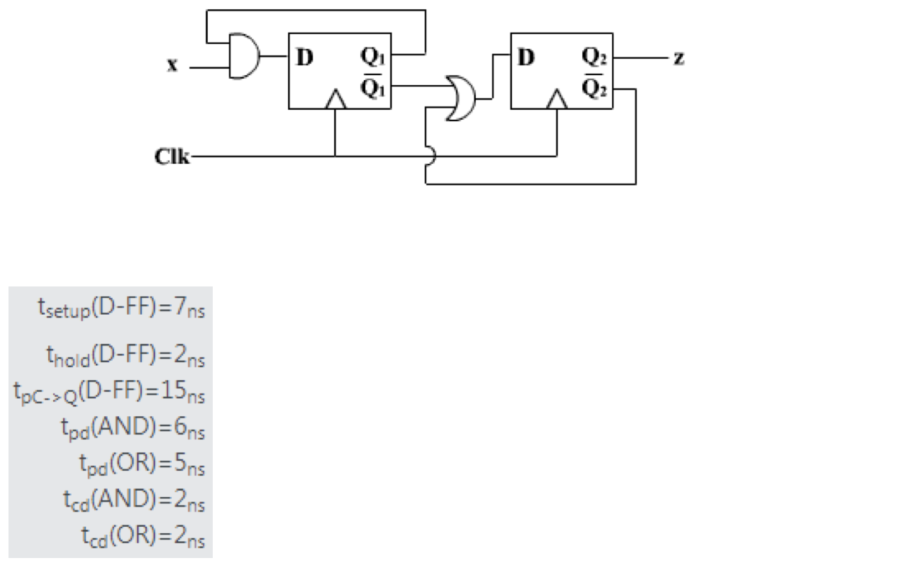
what's the minimal value of clock cycle time so that the circuit works
with no problems?
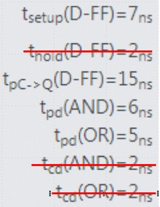
Clearly, Setup is the relevant one for the analysis. Because Hold has no relation with clock period. However, you can crosscheck Hold in all paths with the given values to make sure that no path has hold violation.
For the time being, ignore the input-to-FF path from x to FF1.
Consider the rest of the three FF-to-FF timing paths -
- \$\text{Clk-to-Q1} \rightarrow \text{AND} \rightarrow \text{FF1} \$
- \$\text{Clk-to-}\overline {Q1} \rightarrow \text{OR} \rightarrow \text{FF2} \$
- \$\text{Clk-to-}\overline {Q2} \rightarrow \text{OR} \rightarrow \text{FF2} \$
From given values of propagation delays, the worst-delay path (critical path) is -
- \$\text{Clk-to-Q1} \rightarrow \text{AND} \rightarrow \text{FF1} \$
Setup analysis for that path -
$$T_{clk\rightarrow Q_1}+T_{pd(AND)}+T_{setup}\le T_{clk}$$
$$\implies 28 \text{ ns} \le T_{clk}$$
This COULD be the minimum the clock period of the clock. But to conclude it, you have to see the requirement at the input path to FF1 from x. It has to satisfy the timing as well for \$T_{clk} = 28 \text { ns.}\$ Otherwise, it could be the critical path. This path is -
- \$\text{input at x} \rightarrow \text{AND} \rightarrow \text{FF1}\$
Setup analysis for this path -
$$T_{in}+T_{pd(AND)}+T_{setup}\le T_{clk} \tag 1$$
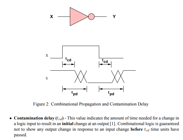
It's known that the time between positive-edge and negative-edge of the clock (which comes after) is required to be 13 ns or bigger. And that the input X gets updated when the clock reaches negative-edge.
The meaning of this is, the input delay at x has to be assumed as 13 ns at least. So if we plug in value 13 ns in equation (1) -
$$\bbox[6px,border:1px solid green] {26\le 28 \text { ns}} \text { -- satisfies!}$$
Initial Conclusion
If the input delay at x becomes > 15 ns for instance, it becomes the critical path, and the minimum clock period will then have to be more than 28 ns. So the minimum clock period in which the circuit can operate under given conditions is 28 ns.
Exception
Honorable mention to @StainlessSteelRat's answer, +1. Consider our critical path - \$\text{Clk-to-Q1} \rightarrow \text{AND} \rightarrow \text{FF1} \$
Actually if the flip-flop FF1 has no preset input, there is no way Q of FF1 to become 1 in the given circuit. Or in other words, this path never toggles. This kind of path is called False Path in digital designs. False paths can always be safely ignored in timing analysis as it can be pessimistic for setup analysis (especially in this particular circuit).
Final Conclusion
Considering the false path into picture, the critical path now becomes any of the remaining two timing paths. Both have 27 ns delay. And this clock period still satisfies equation (1). So the minimum clock period in which the circuit can operate under given conditions is 27 ns.
You can point out this to your professor, maybe he missed out this.


